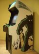
Modding a NES to run Unisystem VS arcade games
- The idea
- Differences between the NES and the Unisystem VS
- Step 1: Deactivating the lockout chip
- Step 2: Additional memory for the PPU
- Step 3, Additional memory for the CPU
- Step 4: ROM for the CPU (PRG-ROM)
- Step 5: ROM for the PPU (CHR-ROM)
- Step 6: Additional wiring due to cartridge absence
- Step 7: Button for coin insertion
- Step 8: Dip switches
- Palette fix patch
- Combining the roms
- Ressources
- Disclaimer
The idea

 At work, we did a high scores competition at Super Mario Bros,
arcade version (Unisystem VS). My score was not high enough so I decided
to train using the NES version at home. After playing a few minutes, I
discovered that there was many differences between the NES and Arcade version
of Super Mario Bros.
At work, we did a high scores competition at Super Mario Bros,
arcade version (Unisystem VS). My score was not high enough so I decided
to train using the NES version at home. After playing a few minutes, I
discovered that there was many differences between the NES and Arcade version
of Super Mario Bros.In the arcade version, there are less mushrooms (
 ),
less flowers (
),
less flowers ( ), and
less lives (
), and
less lives ( ). They are usually
replaced by coins or nothing. Some monsters are changed, there
are more pits and some levels are completely different. The arcade
version is harder!
). They are usually
replaced by coins or nothing. Some monsters are changed, there
are more pits and some levels are completely different. The arcade
version is harder!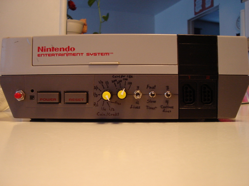 Instead of practising using the Mame emulator, I decided to mod
a NES console to make arcade roms playable on it. I could also
have built a cartridge but modding the console was more fun and I
learned a bit more. I wonder what's more fun: Playing the game or modding
the console? ...
Instead of practising using the Mame emulator, I decided to mod
a NES console to make arcade roms playable on it. I could also
have built a cartridge but modding the console was more fun and I
learned a bit more. I wonder what's more fun: Playing the game or modding
the console? ...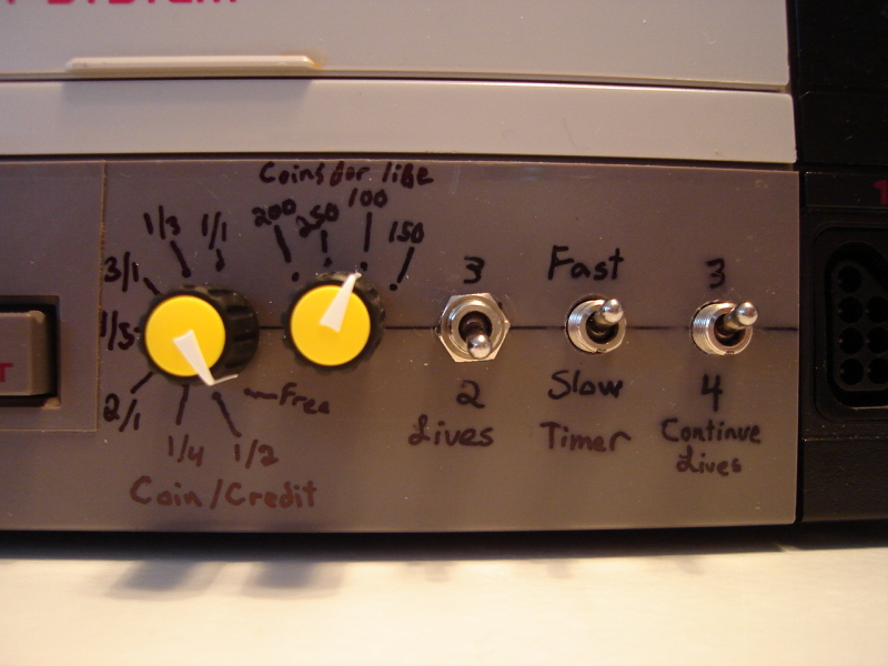 The result: A dedicated Super Mario Bros VS. console, without
a cartridge (no bad contacts) with switches on the front panel to tweak
some aspects of the game (A user friendly version of dip switches found
on the arcade motherboard).
The result: A dedicated Super Mario Bros VS. console, without
a cartridge (no bad contacts) with switches on the front panel to tweak
some aspects of the game (A user friendly version of dip switches found
on the arcade motherboard).
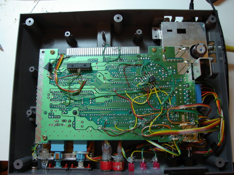
On the following page, you'll find pictures and explaination about what I did to obtain these results. And it's not only electronics...
Differences between the NES and the Unisystem VS
If you'd like to compare the two systems by yourself, here are the schematics: Unisystem VS schematic
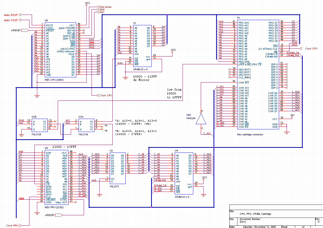
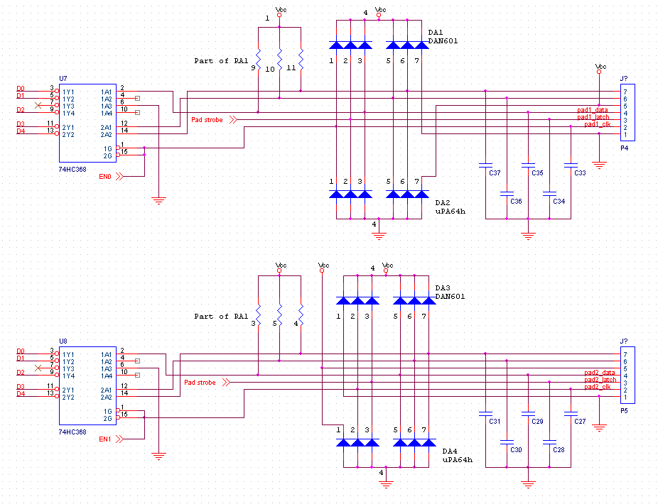 NES CPU, PPU, Memory and cartridge connector.
NES input circuitry (controllers) schematic.
The Unisystem VS arcade motherboard is like two NES on the same board, without cartridges (the roms are on-board).
A few things the NES and Unisystem have in common:
- The same CPU (2A03) is used. (The 2A03 is a modified 6502)
- The PPU is register compatible.
- Same memory map.
- Controller buttons are read the same way.
- The PPU color palette is different. The NES uses a 2c02 PPU. The Unisystem uses other PPUs such as the 2c03, 2c04 and 2c05. All of them have different color palettes. (But I think the 2c02 and 2c03 have similar palettes).
- The arcade PPUs have RGB outputs instead of composite. (RGB is much better!)
- The arcade motherboard has dip switches to configure the game (Number of lives, credits per coin, etc...)
- The unisystem has an input connected to a coin acceptor.
- The two systems on the Unisystem motherboard can communicate together
- The Unisystem does not have a lockout chip.
This is not possible on an Unisystem VS since the roms are installed directly on-board. The games must use the ressources available on-board. Here's what's available:
- Program ROM from $8000 to $FFFF. (Identical to the NES)
- Additional memory from $6000 to $7FFF. (Some NES games provide this)
- 2 16Kb ROM for the PPU, Selected by the CPU using a spare output. (Possible on a NES but I dont know any game which does this.)
- There is 4Kb of memory installed for the PPU instead of only 2Kb. (Some NES games provide this too)
Step 1: Deactivating the lockout chip
 The NES's lockout chip normally communicates with another lockout chip inside
the cartridge. Since there will be no cartridge it will need to be disabled. This
can be done by disconnecting pin number #4 (just cut it) and connecting it to ground. For
more details, read my
NES stuff
page.
The NES's lockout chip normally communicates with another lockout chip inside
the cartridge. Since there will be no cartridge it will need to be disabled. This
can be done by disconnecting pin number #4 (just cut it) and connecting it to ground. For
more details, read my
NES stuff
page.Step 2: Additional memory for the PPU
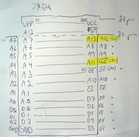
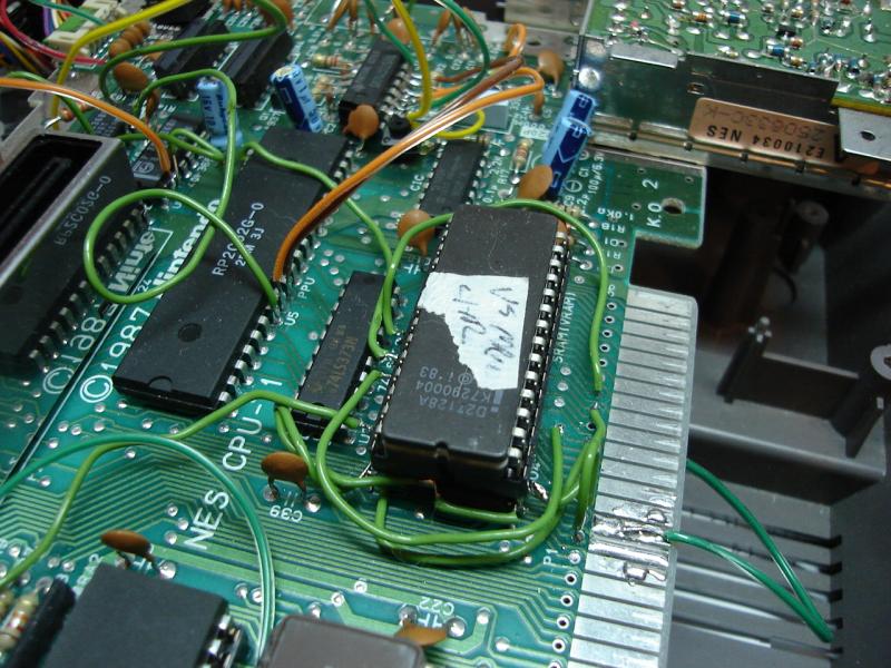
As I explained previously, 4KB of memory must be available to the PPU instead of 2KB. The memory chip (U4) must be replaced by a bigger one.The pinout uesd by different memory chips is usually similar. This allows us to solder the bigger chip where the small one was, with a minimal number of wires and bent pins. The additional address line A11 must be connected to PPU pin #27. If you use a memory chip bigger than 4K, connect all the remaining address pins (A12 and higher) to VCC or ground.
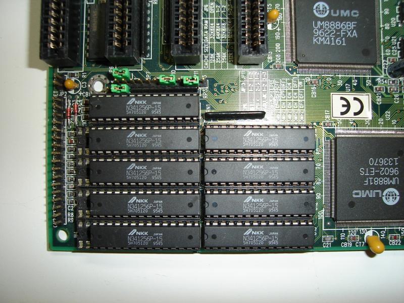
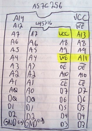 On an old 486 motherboard, I found an As7c256 32K
sram chip. To make sure I did not make mistakes, I drew a small diagram to compare
the pinout of the 2K memory chip (LH5216) with this new chip.
On an old 486 motherboard, I found an As7c256 32K
sram chip. To make sure I did not make mistakes, I drew a small diagram to compare
the pinout of the 2K memory chip (LH5216) with this new chip.
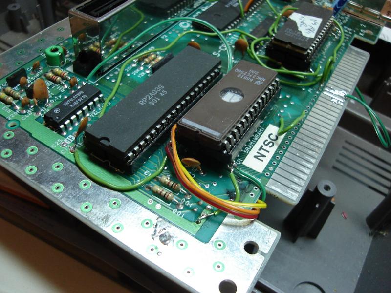
Step 3, Additional memory for the CPU
 The Unisystem VS provides 2KB of additional memory to the CPU. I took the
2KB chip (LH 5216) I removed from the PPU in the previous step and soldered it
under under the other CPU memory (U1) by bending all the pins upwards.
The Unisystem VS provides 2KB of additional memory to the CPU. I took the
2KB chip (LH 5216) I removed from the PPU in the previous step and soldered it
under under the other CPU memory (U1) by bending all the pins upwards.The /CE (Chip enable) pin is not soldered since this memory must be accessible from $6000 to $7FFF. Pin #7 of the 74ls139 present on the NES motherboard happends to be low during this range so I connected it to the additional memory's /CE pin.
Step 4: ROM for the CPU (PRG-ROM)
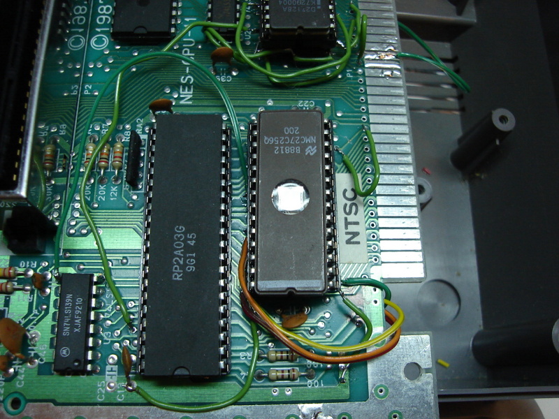 The Unisytem VS uses 4 8KB roms for the CPU (PRG-ROM). I did not want to install
4 sockets and hundread of wires so I decided to use a single 32KB eprom. To ease
installation even more, I simply soldered on top of the CPU's memory chip (U1). The /CE signal
is connected to pin #3 of the 74ls139 (U3) so the ROM is accessible from $8000 to $FFFF.
The Unisytem VS uses 4 8KB roms for the CPU (PRG-ROM). I did not want to install
4 sockets and hundread of wires so I decided to use a single 32KB eprom. To ease
installation even more, I simply soldered on top of the CPU's memory chip (U1). The /CE signal
is connected to pin #3 of the 74ls139 (U3) so the ROM is accessible from $8000 to $FFFF.Again, I used a diagram to compare the ROM and memory pinout. Be careful, this diagram is for a 27128 (16K) eprom instead of a 27256. On a 27256, pin #1 is A14 and on a 27128, pin #1 is VPP.
Step 5: ROM for the PPU (CHR-ROM)
 The Unisystem VS has 2 8K roms available for the PPU. The CPU pin #37 controls
which ROM is usable. Still not wanting to use two sockets and about 32 wires, I decided
to use a single 16K eprom. Since I only have one eprom, I connected CPU pin #37 to A13. The
/CE signal is connected to the PPU A13 signal directly.
The Unisystem VS has 2 8K roms available for the PPU. The CPU pin #37 controls
which ROM is usable. Still not wanting to use two sockets and about 32 wires, I decided
to use a single 16K eprom. Since I only have one eprom, I connected CPU pin #37 to A13. The
/CE signal is connected to the PPU A13 signal directly.I soldered the ROM on top of the PPU memory. Again, I used a small diagram to compare the ROM and memory pinouts.
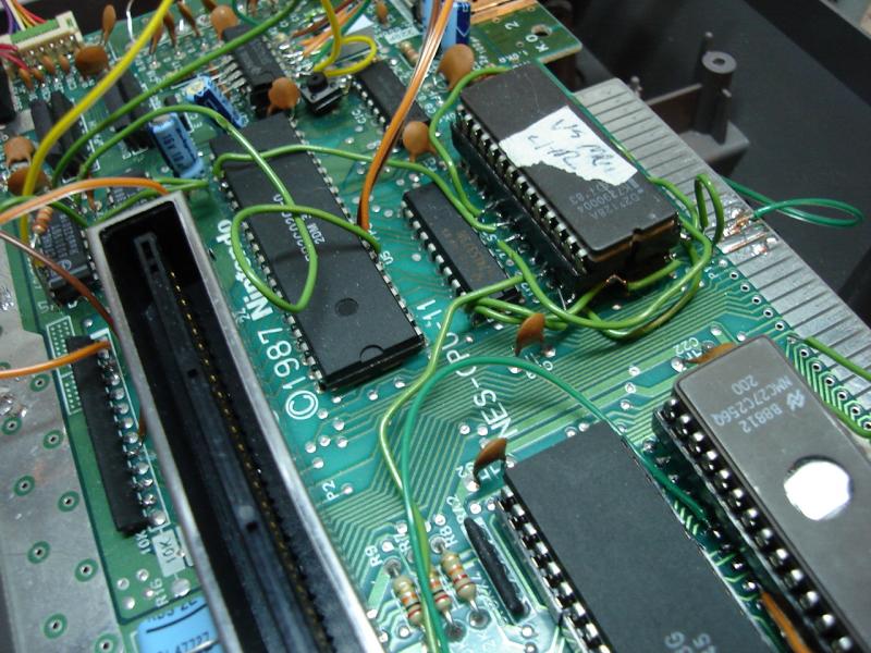
Step 6: Additional wiring due to cartridge absence
1: The PPU memory /CE signal is usually controlled from an inverted A13 signal (inverted by U9, pins 5 and 6) and passes through the cartridge. This allows a cartridge to provide their own PPU memory and to disable the internal memory. Since we dont have any cartridge, contacts #58 (CHR /A13) must be connected to contact #57 (ciram /CE).2: The A10 signal that goes to the PPU memory does not come directly from the PPU. It goes through the cartridge too. By connecting memory signal A10 to PPU A10 or A11, the cartridge can choose between horizontal and vertical mirroring. Since we have 4KB of memory, mirroring is not applicable. Just connect contact #62 (CHR A10) to contact #22 (CIRAM A10).
Step 7: Button for coin insertion
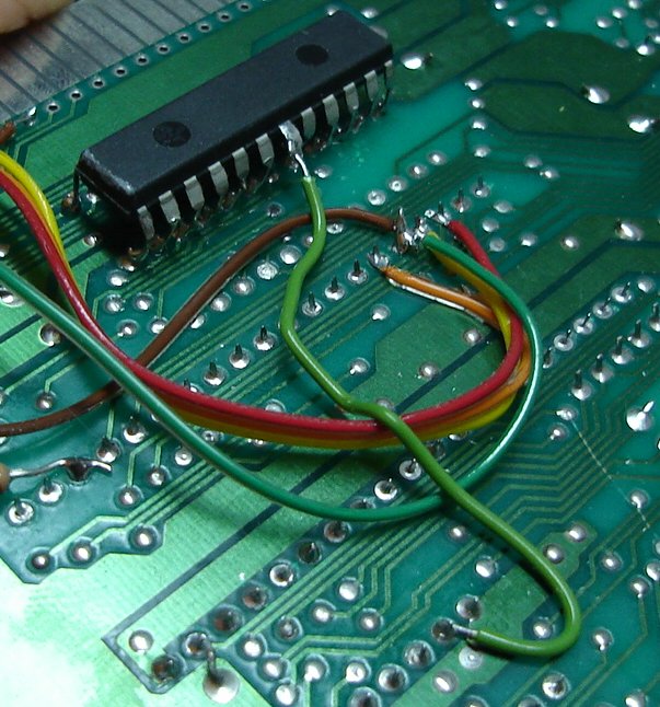
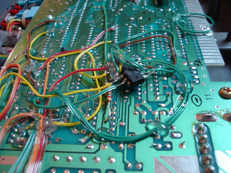
The Unisystem VS has an input normally connected to a coin acceptor. Electrically, the coin acceptor is similar to a button.The game monitors bit 5 at address $4016 (same address as first controller) for pulses coming from the coin acceptor. When this address ($4016) is read, cpu pin #36 goes low. When this occurs, the 74hc368 (U7) takes control of a few data signal on the BUS. D5 however, is left floating.
In order to drive D5, we can use a spare gate of U7. Cut the track connecting pin #6 to ground and install a pull-up resistor of about 10k on it. Next, connect this pin to a momentary switch (or to a real coin acceptor) which will connect to ground when pressed. Finally, connect U7 pin #7 to the CPU D5 signal.
Here is a picture explaining those steps:

Consult the Unisystem VS schematic and the NES input circuits schematics for more details.
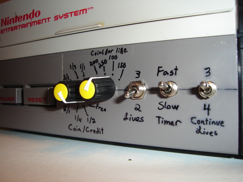
Step 8: Dip switches
The Unisystem motherboard has dip switches to configure some parameters of the game. The game can read those switches using addresses $4016 and $4017, one bit per switch. Here is a table showing which bit and address is used by each switch, where we can connect them in a NES and what they do in Super Mario VS:| Dip | Address | Bit | Connection point | Fonction |
|---|---|---|---|---|
| Dip 1 | $4016 | Bit 3 | P4, pin #7 | Sets the
Coin/Credits ratio: 3/1, 2/1, 1/1, 1/2, 1/3, 1/4, 1/5 or free play. |
| Dip 2 | $4016 | Bit 4 | P4, pin #6 | |
| Dip 3 | $4017 | Bit 2 | U8, pin #10 | |
| Dip 4 | $4017 | Bit 3 | P5, pin #6 | New game lives. 2 or 3. |
| Dip 5 | $4017 | Bit 4 | P5, pin #7 | Number of coins required to obtain a new life. 100, 150, 200 or 250 |
| Dip 6 | $4017 | Bit 5 | Use a buffer which will be in tri-state when CPU pin #35 is not low and connect outputs to CPU pins D5, D6 and D7. I used a 74ls125 but a 74ls244, 74ls240 or 74hc368 from another NES would work too. | |
| Dip 7 | $4017 | Bit 6 | Timer speed. Fast or slow. | |
| Dip 8 | $4017 | Bit 7 | Lives after a continue. 3 or 4. |
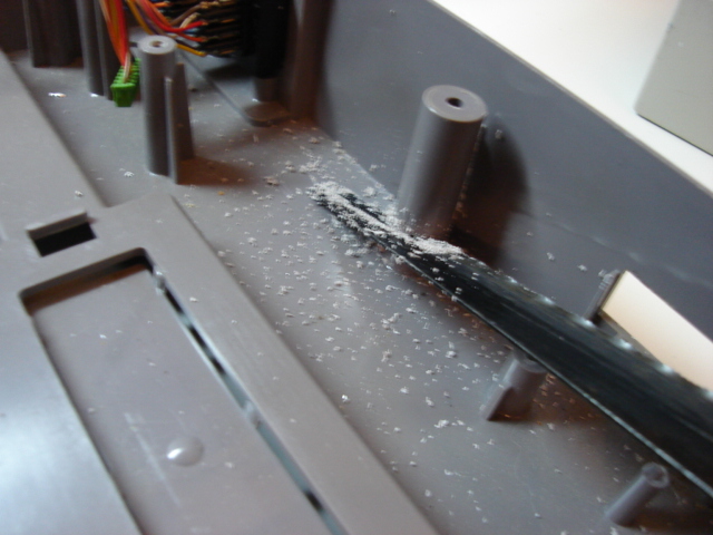
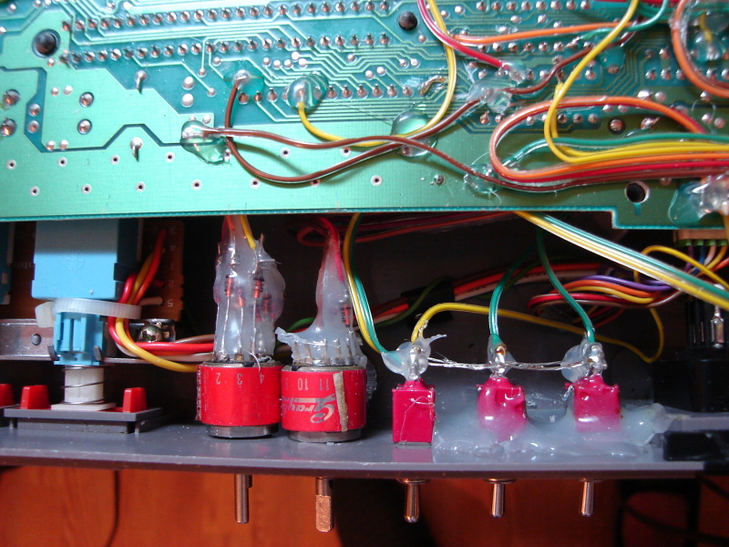
For parameters which use more than one switch, I used rotary switches. Simple diode circuits convert the rotary switch output to binary. In order to have enough space for all those switches on the front panel, I had to cut some plastic:
Palette fix patch
The PPU used by the arcade version of Super Mario Bros (2c05) is not the same as in the NES. They are compatible but the color palette is different. Here is what the arcade version looks like on a NES ppu (2c02):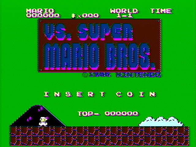
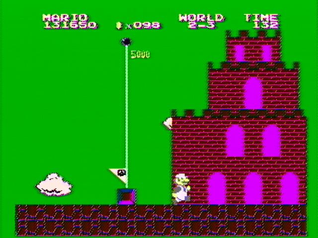
The PPU registers from $3f00 to $3f1f (mirrored from $3f00 to $3fff) holds the 16 currently selected colors for the background and the 16 currently selected colors for the sprites. Each byte represents a color number. Their meaning differs between different PPU. eg: Color $1a on a 2c05 is blue while on a 2c02 it's green!
To correct this problem, I created a rom patch to make sure the right colors are sent to the PPU. Here is how I did:
- I converted the Unisystem ROM files to a .NES in order to be able to use them with NES emulators and debuggers. (Note: Use mapper 99)
-
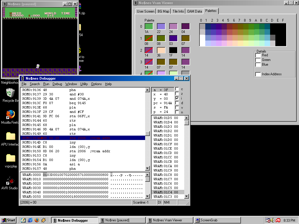
 I used No$NES
(a NES debuger) to find the subroutine which transfers the palette to the PPU. The
subroutine starts at address $914a. It expects a pointer (located at $0000)
to a transfer structure. This copy structure containts the destination PPU address,
the length of the copy and the data.
I used No$NES
(a NES debuger) to find the subroutine which transfers the palette to the PPU. The
subroutine starts at address $914a. It expects a pointer (located at $0000)
to a transfer structure. This copy structure containts the destination PPU address,
the length of the copy and the data.
The copy subroutine works like this:- Send the destination address to the PPU.
- Send all the data to the PPU.
- Return
- I found what I think is an empty space in the ROM (all $FF during 148 bytes) big enough to hold my code and a color conversion table. I used a conversion table from the AdvanceMame. emulator source code.
- In the copy subroutine, I inserted a jump (JMP) to my code just before the copy loop. Since the copy subroutine is not only used for palette data, my code checks the destination address. If the destination address is not in the palette range, I jump back to the normal copy loop. If the destination address is in the palette range, my copy loop is executed. All the data is then copied and corrected on-the-fly using the conversion table.
How to apply the patch:
Here is a file which you must be placed at address $159C in the file mds-sm4.1d: fix_palette.bin
Next, in mds-sm4.1d, replace the 3 bytes $4A $4A $AA (lsr A, lsr A, txa) at address $116B by $4C $9C $95 (jmp $959c).
Here is the source code. I use wla dx since I can use it under Linux:
fix_palette.asm
NOTE: Dont bother asking me for the ROMS or where to get them, I wont reply.
Combining the roms
Unisystem VS games roms come in separate files, just as the EPROMs on a real motherboard. Since I use only one EPROM, I must combine all the rom files in a single one. It's easy, but the files must be combined in the right order.If you look at the Unisystem VS schematic, you will see that the roms are mapped in memory like this:
- 1D: $8000 to $9FFF
- 1C: $A000 to $BFFF
- 1B: $C000 to $DFFF
- 1A: $E000 to $FFFF
# cat mds-sm4.1d > mds-sm4.bin
# cat mds-sm4.1c >> mds-sm4.bin
# cat mds-sm4.1b >> mds-sm4.bin
# cat mds-sm4.1a >> mds-sm4.bin
The same concept applies to the PPU roms: 2B comes first, then 2A.
NOTE: Dont bother asking me for the ROMS or where to get them, I wont reply.
Ressources
I found these documents or websites extremely useful while doing this mod:Documents:
NES PPU Technical reference
Deactivating the lockout chip
NES cartridge info
Links:
nesdev.parodius.com The best site for NES information.
Schematics:
NES CPU, PPU, Memory and cartridge connector schematic.
NES input circuitry schematic.
Unisystem VS schematic
Disclaimer
I cannot be held responsible for any damages that could occur to you or your equipment while following the procedures present on this page. Also, I GIVE ABSOLUTELY NO WARRANTY on the correctness and usability of the informations on this page. Please note, however, that the procedures above have worked in my case without any damages or problems.Now you cannot say that I did not warn you :)